A primary goal of our business is not just to provide a solution to your specific application, but also allow you to learn. The purpose of this page is to provide information regarding technology components, history and procedures plus terms which you may encounter. This page currently covers the history and basics of microprocessors and memory parts plus bios chip history and in-circuit programming information. The page will be updated as more subject material is available. Please review the information. Use the navigation menu on the right to select any item in which you have interest. We hope you find it useful.
How is the EPROM organized inside?
The
EPROM, like any memory chip, is designed to store
individual bits of information. The bit (short for Binary Digit) is the smallest
numeric element used in a computer and can have the value of 0 or
1. This is called binary because the bit can only have two
states. Groups of bits are called by
different terms. Sixteen (16) bits together is called a WORD.
Eight (8) bits together is called a BYTE.
Four (4) bits together is called a NIBBLE.
Obviously a single bit can only represent two states,
therefore it will take multiple bits used together to
represent items such as letters and numbers. The most
common grouping of bits is the byte. Since there are 8
bits and each can be a 1 or 0, there are 256 possible
combinations of 1's and 0's which can be arranged from
the 8 bit grouping.
The typical EPROM is organized as a sequence of bytes
(8 bit groups). Each byte resides at a specific location
in the EPROM called an ADDRESS. The
first address in the EPROM is address 0. The last address
in the EPROM is determined by the EPROM storage capacity.
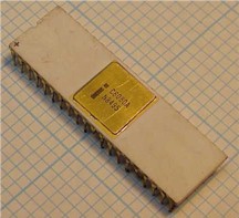
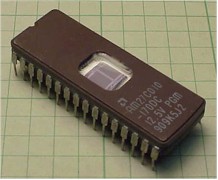
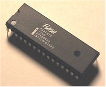
The EPROM in the photo is a 27C010. It has a storage
capacity of 128K (1FFFF hex) bytes. When a CPU accesses the EPROM, it provides an ADDRESS to the chip and then reads the BYTE from
that address. If the BYTE is an instruction, the CPU
decodes the 1's and 0's in the byte and performs the
operation the instruction specifies. This is how the
EPROM stores a program. The CPU sequentially
addresses each byte in the EPROM to get the instructions
which allow the computer to do its job. The illustration
above shows eight addresses and corresponding data. The
data values are shown in BINARY (left) and HEX (right).
HEX is a more compact form of presenting binary numbers.
HEX numbers are described later in this page.
EPROM
ORGANIZATION
| ADDRESS 0 |
01001000
(48) |
| ADDRESS 1 |
00000010
(02) |
| ADDRESS 2 |
11000110
(C6) |
| ADDRESS 3 |
11100000
(E0) |
| ADDRESS 4 |
11110001
(F1) |
| ADDRESS 5 |
00011111
(1F) |
| ADDRESS 6 |
10011001
(99) |
| ADDRESS 7 |
00000000
(00) |
What does the part number mean?
The
EPROM part number normally indicates the total number of
bits of storage in thousands. For example, a 27256 EPROM
has 256,000 bits of storage. If you divide 256,000 by 8
(number of bits in a byte) you get 32,000 or 32K (K is an
abbreviation for kilo or thousand). Please note that not
all EPROM part numbers represent the number of bits. For
example the 27C040 stores 4 million bits or 512K bytes of
data.
What is EPROM
speed?
The speed specification for an
EPROM is actually a specification for access time. The
access time is the time it takes the EPROM to deliver the
data from the requested address to the CPU. The
access time is specified in nanoseconds (billionths of a
second). The access time is usually found following the
part number. Example: M5M27C64A-25 is a
27C64 EPROM with a 250 nanosecond access time. The access
time is normally found after the dash (-) which separates
the part number from the access time. When you replace an
EPROM or any memory device, you may substitute a part of
equal or faster speed but not one of slower speed. Example: You can replace a 27C64A-25 with a 27C64A-20 but not with
a 27C64A-30. The data can be available from the EPROM
before it is needed however if the CPU attempts to
take the data before it is there, the product the
computer is in will not work.
Figuring out the part number on
your chip
EPROMs and most other memory parts conform to a
standard pin configuration and operate in an identical
manner. This allows parts from any manufacturer to be
used interchangably. The key is to figure out the part
number on your device. Usually the part number is printed
directly on the top of the part. What you are looking for
is the core part number.
This is the industry standard number for the part. The
typical EPROM is a 27 series device. EPROMS compose about
80% of the programmable memory device market. Regardless
of who manufactured the part, the part number should have
27XXX or 27CXXXX printed somewhere on the device. This
number may have a prefix or suffix associated with it. An
example would be the HITACHI 2716 EPROM. The part number
on the chip is HN42716G. Note where the 2716 appears (HN4 2716G).
An identical part made by National Semiconductor is
numbered as NMC27C16Q-35 where a part manufactured by
Intel is D2716-1. Don't get confused by a date code. A
date code is printed on the chip to indicate when it was
manufactured. A date code is the year of manufacture
followed by the week. An example would be 8925. This
indicates that the part was manufactured in the 25th week
of 1989. Although a date code is not easily confused for
a 27XXX chip, it can be for other types of memory parts
which are not 27XXX devices.
Erasing an EPROM and the window
The
information (bits) which compose the data in the EPROM are stored as an
electrical charge on a transistor arary in the EPROM itself. There is
one transistor for each bit of storage. The programming
process forces the charge on the transistor where it
remains trapped until the part is erased. A charged
(programmed transistor) holds the bit value of 0 where an
erased (unprogrammed transistor) holds the bit value of
1. Once a transistor in the EPROM is programmed, the only
way to remove the trapped charge is to expose the entire
chip to high intensity ultraviolet light using an EPROM ERASER.
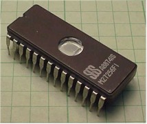
If you look at a standard EPROM you will see that it has
a clear window in the center of the part. The purpose of
this window is to allow the ultraviolet light to reach
the transistors which compose the EPROM memory array and
dissipate the electrons trapped on the transistors.
Usually an EPROM, once it has been programmed, will
have a cover or sticker placed over the window. You
cannot erase an EPROM or change its contents by removing
this cover and exposing it to normal room light. Even in
direct sunlight it would take two weeks of constant
exposure to alter the chip. You cannot erase an EPROM
with a black light or tanning bed, it is best to use an
eraser manufactured to erase EPROMs and other
programmable devices.
EPROMs in plastic packages
A
very expensive part of the EPROM is the ceramic package
with the quartz window. All manufacturers provide their
EPROM products in plastic packages without windows. These
are called OPT (One Time
Programmable) devices simply because there is no
window to erase the part. There is nothing to prevent an
OTP device from being read and the contents placed into
another EPROM. OTP devices are standard EPROMs which can
only be programmed and used once. The part number is
usually something such as P27CXXX where the "P"
indicates a plastic case.
What is the difference between a
27 and a 27C part?
The 27XXX EPROMs use
the first memory cell technology. The technology process
is called NMOS. NMOS stands for "N-channel"
"Metal" "Oxide"
"Semiconductor". The next
generation technology is called CMOS, thus the letter
"C" in the part number. CMOS stands for "Complimentary"
"Metal" "Oxide"
"Semiconductor". CMOS parts
use much less power than NMOS parts, however all other
aspects of the devices are identical. You can substitute
a CMOS for an NMOS part with no problems, however since
an NMOS part consumes more power, it is not advisable to
put an NMOS part in place of a CMOS. This is especially
true in battery powered equipment.
Different package types
There are several package types into
which memory parts or microcontrollers are found. The
traditional package, which has been shown throughout this
page, is called a DIP. DIP stands for "Dual" "Inline"
"Package". It is so called
because it has two rows of pins which insert into a
socket or holes in the circuit board. The primary
advantage of this package is that it is easily removed
and installed by humans. In reality, the actual memory
chip is much smaller than the package into which it is
placed. DIP packages can be of any size between 8 and 42
pins. Typical EPROMs are normally found in 24, 28 or 32
pin packages depending on device storage capacity. There
are 16 bit EPROMs which are found in 40 pin packages. The
40 pin package is used because the data is read 16 bits
at a time and thus requires more physical pins to connect
to the processor.
In order to conserve space
there are several package styles which have become
common. One is the PLCC. PLCC stands for "Plastic" "Leaded"
"Chip" "Carrier".
A PLCC package is physically smaller than a DIP and has
leads on all four sides. The most common size for EPROMs
is 32 pins, although smaller and larger PLCC packages are
not uncommon. PLCC packages have the primary advantage of
size. With electronic products becoming increasingly
small, designers use PLCC parts for surface-mount or
space limited designs. There are sockets available for
PLCC parts, however they require a special tool to remove
the device. If the PLCC part is soldered directly to the
board, the part must be desoldered before it can be read.
A special adapter is required to use a PLCC part with a
device programmer. The adapter performs the conversion
from the PLCC package to a traditional DIP base.
A second space conserving package style is the SOIC or PSOP. SOIC stands
for "Small" "Outline"
"Integrated" "Circuit".
PSOP stands for "Plastic" "Small"
"Outline" "Package".
SOIC/PSOP devices have leads on only two sides and as
such are similar to a DIP although much smaller.
SOIC/PSOP packages may also be installed in a socket,
although they are usually soldered directly to the
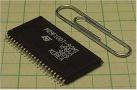
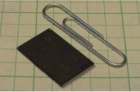
circuit board. The device shown in the photo is a 29F100T
flash memory part. A special clam-shell style adapter is
required to support SOIC/PSOP devices which insures
proper lead alignment and connection.
One of the smallest package styles available is the TSOP. TSOP stands for "Thin"
"Small" "Outline"
"Package". These devices are
always soldered to the board and are also found in FLASH
MEMORY CARDS and other space critical applications. A
special adapter is required to support these devices. The
adapter socket has tiny retractable contacts which mate
with each fine-pitch device lead.
ADDITIONAL PROGRAMMABLE MEMORY PARTS
FLASH
EPROMS
Flash EPROMs are the most
recent type of EPROM memory part. These parts are always
in plastic cases because the erasing of the part is done
electrically without the need to expose the internal chip
to ultraviolet light. The erase function is performed by
the EPROM programmer and requires less time than a UV
EPROM to be erased in an eraser. They erase in a " FLASH",
and thus the name. Flash memory parts cannot be
substituted for a standard UV erasable part because the
minimum number of pins on a typical flash part is 32. The
smallest flash device is a 28F256 which is equal in
storage capacity to a 27256 UV EPROM. Note the part
number 28FXXX is a FLASH device designated by the
"F" in the part number.
EEPROMS
EEPROMs
are memory parts which use the same technology as an
EPROM, however each bit of storage has extra transistors
to allow the bit to be individually erased. The term
EEPROM means " Electrically"
" Erasable" " Programmable"
" Read Only Memory".
Unlike Flash devices, these memory parts can have
individual bytes changed without the need to erase the
entire part. The way this works is that the memory chip
itself performs an erase on a single byte before
programming the byte with the new data. The erase and
program of a single byte can take as long as 10
milliseconds. This delay prevents an EEPROM from
replacing a normal RAM part. An example of a EEPROM is a
28C64. Note that the number 28 is used both for EEPROMs
and FLASH devices. The "C" in the 28C64 part
number means it is made with CMOS technology. EEPROMs are
more costly than EPROMs because they have more
transistors. EEPROMs are normally used for data storage
in a product since they can be "written to" by
the computer.
SERIAL
EEPROMS
A serial EEPROM is created
with the same technology used in larger parallel EEPROMs.
The difference is that a serial EEPROM typically has only
8 pins on the package. This is because the address and
data are sent to and from the chip one bit at a time
using two or three wires. In order for the computer to
read and write the serial EEPROM it must actually send
commands, data and address information via a predefined
communication protocol. This takes more time and is more
complex than dealing with a larger EEPROM, however the
cost and size savings make these parts very popular where
the amount of information which must be stored is small.
There are three serial EEPROM technology families: "Microwire" whose part numbers start with 93. The "I2C BUS" whose part numbers start with 24 and "SPI" (Serial Peripheral Interface). SPI part numbers start with 25 or 95. These parts are very common and used in many applications including automotive.
Serial EEPROMs are also found in surface mount
packages called SOIC. SOIC stands for " Small"
" Outline" " Integrated"
" Circuit". These packages are
very small and are always soldered directly to a circuit
board. Under many circumstances it is possible to connect
to these parts " in-circuit"
and successfully read and program information. 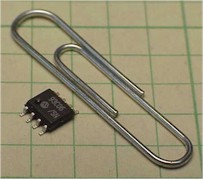
NVRAMS
An
NVRAM is a standard RAM ( RAM stands for
Random Access Memory) which is used for general operation
in computers. The NV stands for non-volatile. The RAM
would normally lose its contents when power is removed,
however the NVRAM is manufactured with a built in battery
which keeps power applied to the memory after power has
been removed from the product. The primary advantage of
an NVRAM is speed. Since the part operates as a normal
high-speed memory part while power is applied, there is
no delay when data is written into the device. There are
also memory parts which are called NVRAMs however they do
not have an internal battery. They maintain there
contents by transferring the data from the RAM memory
array into a duplicate EEPROM memory array. When power is
removed, the EEPROM memory retains the data. When power
is restored, the RAM memory is refreshed to its original
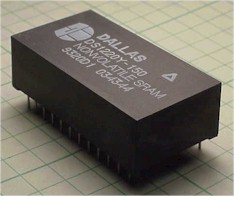
state from the EEPROM array. Example parts of the battery
based NVRAM is the Dallas Semiconductor DS1220(photo) or
DS1225. An example of the EEPROM based NVRAM is the
X22C10 and X22C12 from Xicor.
BIPOLAR
PROMS
A BIPOLAR PROM is a memory
chip which typically contains a small amount of data,
however the access time is very fast. These memory chips
store the bits of data by blowing small fuses inside the
memory device. Once they are programmed they cannot be
changed. The term BIPOLAR reflects the
transistor technology used in the manufacturing process. PROM means "Programmable" "Read Only
Memory". Programming a BIPOLAR PROM requires a high
voltage, high current pulse to blow the fuse. These parts
are found in many products and were a favorite in the
United States Space Program because the data, once
programmed, is immune to changes caused by radiation.
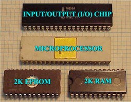
MICROCONTROLLERS
A
microcontroller is a complete computer on a chip. This
includes the central processing unit (CPU), the memory
(EPROM or FLASH EPROM) and the I/O (input/output).
Microcontrollers are usually found in products which
perform a single function such as microwave ovens,
computer printers, automatic sprinkler controllers, etc.
A microcontroller, although much more complex than a
standard memory part, still has internal EPROM/FLASH
EPROM as its program memory. A microcontroller normally
has 40 or more pins since the input and output operations
occur directly from the chip. Some microcontrollers, like
the PIC family from Microchip and others, have fewer I/O
pins and are therefore fabricated in smaller packages.
Since the microcontroller has internal memory, it is this
memory area that you may read and program using a device
programmer. In the past, most microcontrollers used
internal EPROM for their program code and data, however
now all new parts incorporate FLASH memory.
Microcontrollers with FLASH memory are excellent if
you are interested in development since it takes much
less time to erase and reprogram a flash based part than
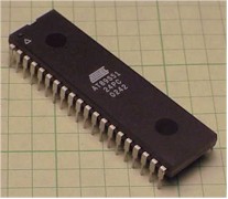
one with UV EPROM. Some examples of 40 pin FLASH
microcontrollers are the ATMEL 89C51, 89S51 and 89C52.
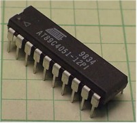
Examples of 18 and 20 pin FLASH microcontrollers are the
Microchip PIC16F84 and ATMEL 89C4051.
WHAT IS HEX?
HEX is short for hexidecimal. Hexidecimal is base 16. Where
humans are used to the decimal system (base 10) with numbers 0
through 9, hex has the digits 0,1,2,3,4,5,6,7,8,9,A,B,C D,E, and
F. Although this may appear confusing, the reason HEX was chosen
is that it provides a simple way to represent 4 binary bits as a
single digit. EXAMPLE: Binary 0000 = HEX 0 or
binary 0101 = HEX 5 or binary 1100 = HEX C. The table below shows
binary numbers and their hexadecimal equivalents.
| BINARY |
HEX |
| 0000 |
0 |
| 0001 |
1 |
| 0010 |
2 |
| 0011 |
3 |
| 0100 |
4 |
| 0101 |
5 |
| 0110 |
6 |
| 0111 |
7 |
| 1000 |
8 |
| 1001 |
9 |
| 1010 |
A |
| 1011 |
B |
| 1100 |
C |
| 1101 |
D |
| 1110 |
E |
| 1111 |
F |
From the above table you can see that if you wish to represent
the binary number 1110010100110010 you can write it as E532 hex.
This is why hex has become the defacto standard to represent and
display binary data; it allows humans to represent large groups
of binary data in a compact form.
WHAT IS ASCII?
ASCII stands for American Standard Code for Information
Interchange. This is a standard translation for HEX (binary)
codes into printable or readable characters. The letters you are
reading on the screen right now are represented in the computer
as groups of bits. Without a standard, any computer manufacturer
could decide which group of bits would represent which letter or
number. In ASCII an upper case A is represented
by the value 41H. the number 3 is represented by the value 33H. When you view
the editor display of a device programmer you should see a
display of HEX information and also (usually to the right) a
display of the ASCII translation of the HEX data. If the data
from an EPROM contains characters which are to be displayed to a
user, these characters will appear in the ASCII display area.
|